Our strong knowledge base, including R&D scientists, engineers, and experienced management, makes Thin Film Processing in sputtering technology possible, delivering solutions of utmost importance to our customers.
Capabilities of our sputtering systems
DC magnetron sputtering , faster metal and dielectric deposition.
RF sputtering to sputter dielectrics and magnetic materials. RF bias for sputter etching and deposition with bias.
Reduced particle counts
Up to 6 different materials without vacuum breaks.
Clean room has micro environments that exceeds class 100 specifications.
Wafer are loaded in FOUP, Cassette, wand depending upon the size and customer requirements.
Film uniformity
The uniformity optimized with the magnetic field configuration
Uniformity can be fine-tuned based on customer requirements to 1 sigma <1%.
Target erosion had no perceivable effect on Thin Film Processing deposition uniformity and thickness.
Lead-Time
Standard production lead-time is less than a week for a majority of Thin Film Processing services.
R&D programs lead-times may be longer depending upon complexity.
Process control Parameters
Process Pressure
Sputter voltage
Substrate Bias
Throw Distance
Substrate temperature
Particle Energy
Characteristics of DSource Dynamic Magnetron Sputter Deposition:
High Deposition Rates 1 micron/min
RF bias for sputter etching and deposition with bias
Water Cooled table for controlled substrate temperature deposition below 40 °C
Batch processing
Almost any metallic target material can be sputtered without decomposition, enabling versatile Thin Film Processing.
Conductive materials can be deposited using a direct current (DC) power supply
Nonconductive materials can be sputtered by using radio frequency (RF)
Oxide, Nitride, and Carbide coatings can be sputtered (reactive sputtering)
Excellent layer uniformity ~ Rs 5%
Better Film Property Control (grain size, stress, etc.)
Cosputtered film depositions available for up to 3 targets
The uniformity is optimized with the magnetic field configuration, ensuring precise control in Thin Film Processing.
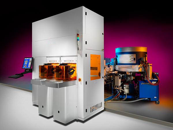
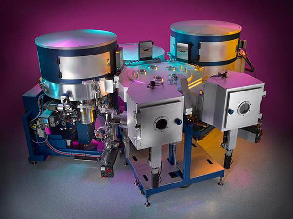
PVD Sputtering
PVD Coating and Thin Film Deposition is the technology of applying a very thin film of material – between a few nanometers to about 100 micrometers. Thin Film Deposition manufacturing processes are at the heart of today’s semiconductor, solar panel, CD, disk drive, and optical device industries. We have in-house tools capable of thin film deposition using D-source magnetron sputtering technology. Magnetron Sputtering is a Physical Vapor Deposition (PVD) process in which a plasma is created and positively charged ions from the plasma are accelerated by an electrical field superimposed on the negatively charged electrode or “target”. The positive ions are accelerated by potentials ranging from a few hundred to a few thousand electron volts and strike the negative electrode with sufficient force to dislodge and eject atoms from the target.
Fully Automated PVD Processing Services:
High strength magnetic array is required for magnetron to saturate the target material and have flux to confine electrons to sustaining plasma
Design of the magnetron is a challenge for achieving full face erosion, uniformity and target life time
Reactive sputter deposition:
Reactive gas, typically, N2 or O2 introduced to chamber during deposition to deposit nitrides or oxides or oxynitrides
Reactive gas, typically, N2 or O2 introduced to chamber during deposition to deposit nitrides or oxides or oxynitrides
Usually done with RF or pulsed DC
Chemical reaction takes place on substrate
Pressure management critical for a good reactive process control of stoichiometry, stress
Metrology
CDE RESMAP:
ResMap Four point Probe, made by Creative Design Engineering (CDE), is a semiautomatic tool to measure the sheet resistance of a thin film or the bulk resistance of a wafer/sample.
The wafer/sample is manually loaded onto the probe platform. Measurements are automatically controlled according to the selected recipe that is preprogrammed.
It is capable of accommodating a wafer up to 12 inches in diameter. The maximum number of measurement sites available is 99, and the measurement pattern can be circular, rectangular, linear along the diameter of the wafer, or in a customized geometry.
The measurement range is from 2 mΩ/□ to 5MΩ/□ with 0.5% accuracy.
Film measurement screenshot provided to show thickness and Rs data for the sample i.e. average, range and standard deviation (1sig/3sig values).
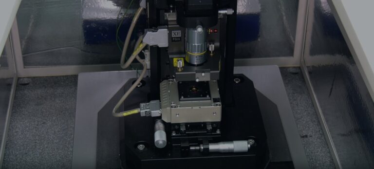
AFM
XE-100 AFM:
The XE-100 AFM (Atomic Force Microscope) is a high-performance atomic force microscope. Equipped with advanced scanning capabilities such as scanning tunneling microscopy (STM), it enables precise surface profiling and analysis of electrical properties.
Measures surface roughness, step heights, and surface profiles with high accuracy.
Provides the topography of thin films.
Sub-nanometer resolution for high-definition imaging.
Measureable sample size is 80 mm × 80 mm, 20 mm thick, and up to 500 g.
FILMETRICS F50:
The Filmetrics F50 can measure the thickness of dielectrics, semiconductors, and thin metal films for thicknesses between 100Å and 450 microns.
Optical constants such as refractive index (n) and extinction coefficient (k) can also be measured on a variety of dielectric films.
Commonly measured films include: semiconductor process films such as oxides, nitrides, resists, and polysilicon optical coatings such as hardness and antireflection coatings flat panel display films such as polyimides, resist, and cell gaps Various coatings used in CD and DVD manufacture.
Films that cannot be measured include very rough films and opaque dielectric films.
X-RAY DIFFRACTION (XRD):
Used to analyze crystallinity of a film
Optical constants such as refractive index (n) and extinction coefficient (k) can also be measured on a variety of dielectric films.
Optical constants such as refractive index (n) and extinction coefficient (k) can also be measured on a variety of dielectric films.
Films that cannot be measured include very rough films and opaque dielectric films.
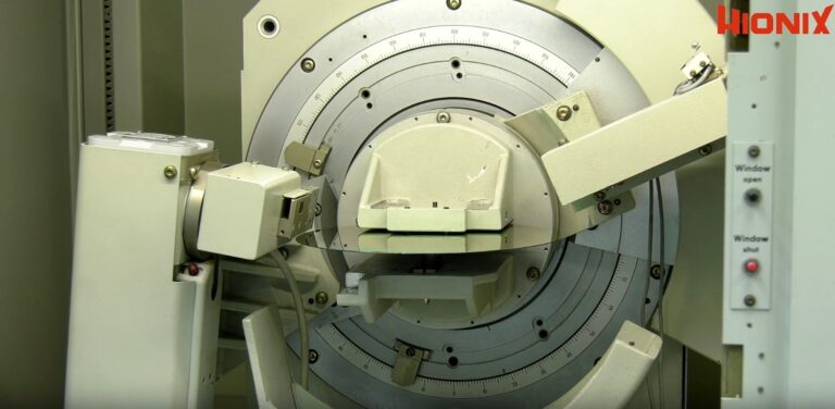
XRD
XRD
Siemens D5000 XRD :
The Siemens D5000 XRD is a non-destructive technique used to analyze and characterize a sample’s crystallography orientation and characteristics.
Used to analyze compounds, crystal structure, crystal orientation, and crystal quality of powder and thin-film samples.
Applications include quantification of crystalline phase, determination of crystallite size, phase identification for thin films, and determination of preferred orientation FWHM
FLX-2320:
The FLX-2300 is a thin film stress analyzer which provides wafer bow and stress data.
Laser Scanning technology is used to measure the radius of curvature and bow of wafers where a laser beam is directed to the wafer.
Simplest and most widely adopted technique in film stress and wafer bow measurement.
The beam is reflected at an angle that corresponds to the radius of curvature of the wafer.
Film stress is calculated from the difference in radius of curvature, i.e. wafer bow, measured before and after deposition of the film.
Stress
A thin film that is deposited on a substrate or is part of a multi-film stack structure will exhibit residual stress that depends on the film thickness. In general, the residual stress of the film, crucial for stress analysis such as Stress Analysis, is defined as the stress that the film will experience when it is in a stand-alone condition or not in contact with any other surface. Film stress is usually classified into two classes:
Intrinsic Stresses:
which represent stress distributions that are present in a film following the deposition / growth step where the film is in contact with a substrate layer or adjacent layers. These are strongly dependent on the process parameters, i.e. chamber conditions, substrate temperature, materials involved etc., which makes them reproducible under the same given conditions.
Extrinsic Stresses:
Those arising from the changes in the external factors affecting the film after the growth / deposition process, i.e. temperature change, chemical reactions, mechanical deformation etc., are also considered in Stress Analysis.
Tensile and Compressive Stress In case of PVD films, residual stress arises because of (a) difference in coefficient of thermal expansion of the film and the substrate at the time of cool down from deposition temperature, and (b) adsorbed atoms not condensing into a state of low energy or equilibrium with one another. Such residual stresses are like stored energy that can be released during subsequent processing steps or with time, emphasizing the importance of stress analysis. For materials with high elastic modulus like Cr, W or metal oxides, very high stresses can be attained with a large amount of stored energy. For low elastic modulus materials like Au or Ag, plastic deformation will occur to relieve stress before high levels of stress are attained.
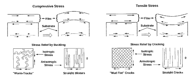
Compressive/Tensile Stress
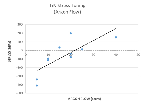
TiN Stress Tuning
The distribution of stress along the thickness of the film is important factor in determining the behavior of the film. If the stress is not uniform throughout the thickness of the film, the film will curl up when detached from the substrate. If it is uniform, the film will lie flat. Film under tensile stress will try to contract, bowing the substrate in the process such that the film is on the concave side. If the film is under compressive stress, it will try to expand bowing the substrate such that film is on the convex side. Tensile stress relieves itself through formation of micro-cracks and subsequent peeling of the cracked surface from the substrate. Compressive stress relieves itself by buckling visible in the form of “worm tracks” or “blisters” on the film surface (see graphic below).
Film stress can be tuned from compressive regime into tensile regime by changing key process parameters such as Power, process gas flow (Ar), substrate temperature etc. Below is an example of such process tuning achieved for TiN (Titanium Nitride).